System Overview
The Romi robot is built on a Pololu Romi chassis and controlled using an ST Nucleo development board running MicroPython. The hardware and electrical design emphasizes predictable startup behavior, clean signal routing, and modular interfaces that support incremental development, debugging, and future extension.
Major subsystems integrated into the robot include:
- Dual DC motors with quadrature encoders
- Reflectance-based line sensor array
- Inertial Measurement Unit (IMU)
- Bluetooth communication module
- Battery-powered system with onboard voltage monitoring
Microcontroller and Power System
The system is powered by six AA batteries, routed through a power distribution board (PDB). Battery voltage is supplied to the Nucleo board via the VIN pin. A resistive voltage divider feeds an ADC input, allowing real-time measurement of battery voltage during operation.
This measurement is used to compensate for battery voltage droop in the motor control pipeline, improving repeatability over the duration of a run.
Startup behavior was treated as a primary design constraint. Motor driver enable (nSLP) pins are explicitly controlled in software, and pin selections were chosen to prevent unintended motor motion during power-up or reset. Pull-down configurations and initialization order were carefully managed to ensure safe and predictable behavior.
Motor Driver Interfaces
Each motor is driven using three signals:
- PWM signal for effort command
- Direction signal
- Sleep/enable (nSLP) signal
Hardware timers were selected to generate PWM outputs independently for each motor without conflicting with encoder timers or communication peripherals. Motor enable pins are controlled as standard digital outputs to enforce explicit enable/disable behavior in firmware.
This structure ensures motors remain disabled until the system has fully initialized and the scheduler has started.
Quadrature Encoder Interfaces
Wheel encoders are interfaced using hardware timer encoder modes. This approach offloads quadrature decoding to dedicated timer hardware, providing robust position and velocity measurements with minimal CPU overhead.
Separate timers are used for the left and right encoders to allow fully independent velocity estimation and closed-loop control. Encoder wiring and pin selection were chosen to avoid overlap with PWM, ADC, and communication peripherals.
Line Sensor Array
Line detection is performed using a multi-channel reflectance sensor array mounted at the front of the chassis. Individual sensors are read using ADC inputs distributed across multiple GPIO ports to balance pin availability and minimize conflicts with timers and communication interfaces.
Although only a subset of sensors is used for control during line following, all channels are wired and supported in firmware. This provided flexibility during development and allowed sensor selection and weighting strategies to evolve without hardware changes.
IMU Interface
An IMU is connected via the I2C2 peripheral. Dedicated SDA and SCL pins were selected to avoid interference with timers, ADC inputs, and UART communication.
The IMU is supported in firmware and was used extensively during Lab 0x05 for state estimation experiments. Although it was not relied upon for the final line-following implementation, its integration provided valuable insight into system dynamics and informed later design decisions.
Bluetooth Communication Interface
A Bluetooth module provides wireless communication between the Romi and a PC. The module is connected via a UART interface and is used for real-time data streaming, diagnostics, and parameter adjustment during testing.
Streaming is enabled by default on startup and can be toggled through the PC-side interface. This approach reduced onboard memory usage and provided immediate visibility into system behavior during controller tuning and debugging.
Pin Assignment Summary
The following table summarizes the primary electrical connections used in the final system configuration. Wire colors are shown explicitly to aid debugging and reproducibility.
| Cable | Contact | Color | Signal / Module Pin | Nucleo Pin | PDB Pin | Port | AF | Function |
|---|---|---|---|---|---|---|---|---|
| Encoder (Left) | 1 | Blue | Encoder Ch. A | Timer Pin, Ch.1 | ELA or ERA | PA9 | AF1 | TIM1_CH2 |
| 2 | Yellow | Encoder Ch. B | Timer Pin, Ch.2 | ELB or ERB | PA8 | AF2 | TIM1_CH1 | |
| Encoder (Right) | 1 | Blue | Encoder Ch. A | Timer Pin, Ch.1 | ELA or ERA | PC7 | AF2 | TIM8_CH2 |
| 2 | Yellow | Encoder Ch. B | Timer Pin, Ch.2 | ELB or ERB | PC6 | AF2 | TIM8_CH1 | |
| Motor (Left) | 1 | Yellow | Motor Enable | Digital Output | nSLP | PB4 | - | Enable / Sleep |
| 2 | Blue | Motor Direction | Digital Output | DIR | PB3 | - | Direction | |
| 3 | Green | Motor Effort | Timer Pin | PWM | PB5 | AF2 | TIM3_CH2 | |
| Motor (Right) | 1 | Yellow | Motor Enable | Digital Output | nSLP | PC9 | - | Enable / Sleep |
| 2 | Blue | Motor Direction | Digital Output | DIR | PB9 | - | Direction | |
| 3 | Green | Motor Effort | Timer Pin | PWM | PB8 | AF2 | TIM4_CH3 | |
| IMU | - | Red | IMU VIN | - | 5V (CN7) | - | - | Power |
| - | — | IMU 3vo | - | Optional* | - | - | Regulated Output | |
| - | Black | IMU GND | - | GND (CN7) | - | - | Ground | |
| - | Burgundy | IMU SDA | - | - | PB14 | AF4 | I2C2_SDA | |
| - | Gray | IMU SCL | - | - | PB13 | AF4 | I2C2_SCL | |
| - | White | IMU RST | - | - | - | - | Reset | |
| Bluetooth Module | 1 | White | Module RX | Romi TX | - | PB6 | AF7 | UART1_TX |
| 2 | Orange | Module TX | Romi RX | - | PB7 | AF7 | UART1_RX | |
| 3 | Black | Module GND | Romi GND | - | GND (CN7) | - | Ground | |
| 4 | Red | Module VCC | Romi 5V | - | E5V (CN7) | - | Power | |
| Battery / Power | 1 | Black | Divider Ground | GND | - | GND (CN7) | - | Ground |
| 2 | Blue | Divider Node | ADC Input | - | PC2 | - | Battery Sense | |
| 3 | Red | Power to Nucleo | VIN | - | VIN (CN6) | - | Board Power | |
| 4 | Black | PDB Ground | - | GND | - | - | Ground | |
| 5 | Red | PDB Battery Power | - | VSW | - | - | Battery | |
| Line Sensors | - | Red | Power | 3.3V | - | 3.3V (CN7) | - | Power |
| - | Black | Ground | GND | - | GND (CN7) | - | Ground | |
| - | Burgundy | Sensor 1 | ADC | - | PC4 | - | ADC | |
| - | Burgundy | Sensor 3 | ADC | - | PA1 | - | ADC | |
| - | Orange | Sensor 5 | ADC | - | PA4 | - | ADC | |
| - | Green | Sensor 7 | ADC | - | PB0 | - | ADC | |
| - | Blue | Sensor 9 | ADC | - | PC1 | - | ADC | |
| - | Yellow | Sensor 11 | ADC | - | PC0 | - | ADC | |
| - | Orange | Sensor 2 | ADC | - | PA6 | - | ADC | |
| - | Green | Sensor 4 | ADC | - | PA7 | - | ADC | |
| - | Gray | Sensor 6 | ADC | - | PA0 | - | ADC | |
| - | White | Sensor 8 | ADC | - | PB1 | - | ADC | |
| - | Brown | Sensor 10 | ADC | - | PC3 | - | ADC | |
| Bump Sensors | - | Black | Ground | GND | - | GND | - | Ground |
| - | Red | BMP0 | Digital Input | - | PH0 | - | Input | |
| - | Green | BMP1 | Digital Input | - | PH1 | - | Input | |
| - | Orange | BMP2 | Digital Input | - | PC10 | - | Input | |
| - | Burgundy | BMP3 | Digital Input | - | PC11 | - | Input | |
| - | Gray | BMP4 | Digital Input | - | PC12 | - | Input | |
| - | Brown | BMP5 | Digital Input | - | PD2 | - | Input | |
| - | White | Ground | GND | - | GND | - | Ground |
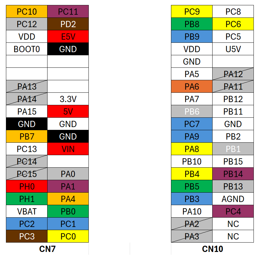
Pinout Reference and Wiring Diagram
The diagram below summarizes the final pin assignments used on the Nucleo board. This diagram was used throughout development to track peripheral usage and avoid conflicts between timers, ADC inputs, and communication interfaces.
Discussion
The hardware and electrical design evolved alongside the firmware throughout the quarter. Careful pin selection, explicit motor enable control, and deliberate startup behavior were critical to achieving reliable and repeatable operation.
By prioritizing modularity and clarity in both wiring and software interfaces, the system remained flexible enough to support experimentation while maintaining a stable configuration for final demonstrations.